Faculty
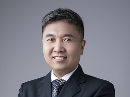
Dr KeiCHEN is now a full Professor , doctoral and postgraduate tutor at the School of Microelectronics at the Southern University of Science and Technology, and executive director of the Engineering Research Center of the Ministry of Education for Future Communication Integrated Circuits. postgraduate courses. Professor Chen Kai graduated from the Department of Electrical Engineering and Computer Science of the University of California, Berkeley, USA, and worked in the Fairchild Research Center and IBM Semiconductor Research Center of National Semiconductor Corporation (now Texas Instruments), and has nearly 20 years of experience in China. Entrepreneurship experience in the United States.. If you are interested in our group, please contact Dr. Chen via email chenk6@sustech.edu.cn.
Education Background
1992 - 1997 USA University of California at Berkeley Electrical Engineering and Computer Sciences (EECS) PhD
1988 - 1989 USA Purdue University Electrical Engineering (EE) Master of EE (MSEE)
1986 - 1988 USA Wayne State University Physics Master of Arts (MA)
1980 - 1985 China Tsinghua University Semiconductor Devices and Physics, B.Eng.
Work Experience
2021 - Present China Professor, School of Microelectronics and Executive Director, Engineering Research Center of Integrated Circuits for Next Generation Communications, Ministry of Education, respectively.
2018 - 2020 China Micro & Nano Electronics National (Key) Lab Preparation Team Leader
2002 - 2017 China Comlent Tech. Inc. Co-founder, Chairman and CEO
2001 - 2002 Hong Kong Authosis Inc. Sr VP and Preisident for Semiconductor Group
1997 - 1999 USA IBM Semicondcutor R&D Center (SRDC) Advisory Engineer
1989 - 1992 USA National Semiconductor Corp. (now Texas Instruments) Sr. Engineer
Major Recognitions
“Annual Top 10 New Comer of China’s Information Industry”
Shanghai Pudong municipal honor“Leaders of Science and Technology”
China’s “25 Most Influential Leaders in IC Decision Making Circle”selected by professional media
Semiconductor Industry Association (SIA) of China’s “Leaders of the Decade”- Leading Entrepreneur Award
Research Interests
Frontier CMOS device physics,device architecture and performance design, device modeling, and process integration, including quantum computing 4.2K-10mK cryogenic temperature CMOS device physics and modeling for circuit design.
Academic Achievement
1. Kai Chen and Chenming Hu, “Performance and Vdd Scaling in Deep Submicrometer CMOS”, IEEE Journal of Solid-State Circuit(JSSC), vol. 33, no. 10, pp. 1586-1589, October 1998;
2. Kai Chen, J.H. Huang, Jon Duster, Ping Ko and Chenming Hu, A MOSFET Electron Mobility Model of Wide Temperature Range (77K-400K) for IC Simulation, Semiconductor Science and Technology, pp. 355-358, vol. 12, no. 4, April 1997;
3. Kai Chen, G. Zhang, J. Duster, J.H. Huang, Z. Liu, P.K. Ko and C. Hu, MOSFET Inversion Layer Capacitance Model Based on Fermi-Dirac Statistics for Wide Temperature Range, IEEE Journal of Solid-State Electronics (ISSE), pp. 507-509, vol. 40, no. 3, March 1997.
4. Kai Chen, Chenming Hu, and Peng Fang, "Optimizing Quarter and Sub-Quarter Micron CMOS Circuit Speed Considering Interconnect Loading Effect", IEEE Transactions on Electron Devices (T-ED), Vol. 44, No. 9, 1997;
5. Kai Chen, Chenming Hu, Peng Fang, and Ashawant Gupta, "Experimental Confirmation of An Accurate CMOS Gate Delay Model for Gate Oxide and Voltage Scaling", IEEE Electron Device Letters (EDL), Vol. 18, No. 6, pp. 275-277, June 1997;
6. Kai Chen, H. C. Wann, J. Duster, M. Yoshida, P. Ko and C. Hu, "MOSFET Carrier Mobility Model Based on Gate Oxide Thickness, Threshold and Gate Voltages", IEEE Journal of Solid-State Electronics (SSE), pp. 1515-1518, Vol. 39, No. 10, October 1996;
7. Kai Chen, C. H. Wann, J. Duster, P. Ko and C. Hu, "The Impact of Device Scaling and Supply Voltage Change on CMOS Gate Performance", IEEE Electron Device Letters (EDL), pp. 202-204, Vol. 17, No. 5, May 1996.
8. Kai Chen, H. C. Wann, J. Duster, P. Pramanik, S. Nariani, P. Ko and C. Hu, "An Accurate Semi-Empirical Saturation Drain Current Model for LDD NMOSFET", IEEE Electron Device Letters (EDL), pp. 145-147, Vol. 17, No. 3, March 1996;
9. Kai Chen, Jian-hui Huang, James Z. Ma, Z.H. Liu, M.C. Jeng, Ping K. Ko and Chenming Hu, "Polysilicon Gate Depletion Effect on IC Performance", IEEE Journal of Solid-State Electronics, pp. 1975-1977, Vol. 38, No. 11, November 1995;
10. Qiuxia Xu and Kai Chen, “Physical Thickness 1.5nm HfZrO Negative Capacitance NMOSFETs”, submitted to IEEE Transactions on Electronics Devices (TED) accepted on 21, 2021;
11. Zhenbiao Li, Wenhai Ni, Jie Ma, Ming Li, Dequn Ma, Dong Zhao, Mehta J., D. Harman, Xianfeng Wang, K.K. O and Kai Chen, “A dual-Band CMOS Transceiver for 3G TD-SCDMA”, Digest of Technical Papers, IEEE International Solid-State Circuits Conference (ISSCC), pages 344-607, Feb. 2007;
12. Isabel Yang, Kai Chen and Lisa Su et al, “Sub-60nm Physical Gate Length SOI CMOS”, IEEE Electronics Device Meeting (IEDM) 1999.
13. Jiqing Lu , Wenhui Wang, Jinxuan Liang, Jun Lan , Longyang Lin,Feichi Zhou, Kai Chen, Guobiao Zhang , Mei Shen, and Yida Li "Contact Resistance Reduction of Low Temperature Atomic Layer Deposition ZnO Thin Film Transistor Using Ar Plasma Surface Treatment," in IEEE Electron Device Letters, vol. 43, no. 6, pp. 890-893, June 2022,doi:10.1109/LED.2022.3169345.
14. Muhammad Zaheer , Aziz-Ur-Rahim Bacha, Iqra Nabi , Jun Lan, Wenhui Wang, Mei Shen, Kai Chen et al, “All Solution-Processed Inorganic, Multilevel Memristors Utilizing Liquid Metals Electrodes Suitable for Analog Computing”,ACS Omega, 22/9/2022.
15. Guobiao Zhang, Hongyu Yu, Shenming Zhou and Kai Chen, “Methods for Making Three-Dimensional Module”. United States Patent and Trademark Office, CONFIRMATION NO.4882 FILING RECEIPT Date Mailed:12/20/2021.


